
In the dynamic landscape of semiconductor manufacturing, efficiency and precision are paramount. The Automatic Wafer Handling System (AWHS) market plays a crucial role in enhancing the efficiency of semiconductor production by automating the handling of wafers throughout the manufacturing process. This market research report aims to provide a comprehensive overview, segmentation, and analysis of the Automatic Wafer Handling System Market, shedding light on key players driving innovation and growth.
Market Overview:
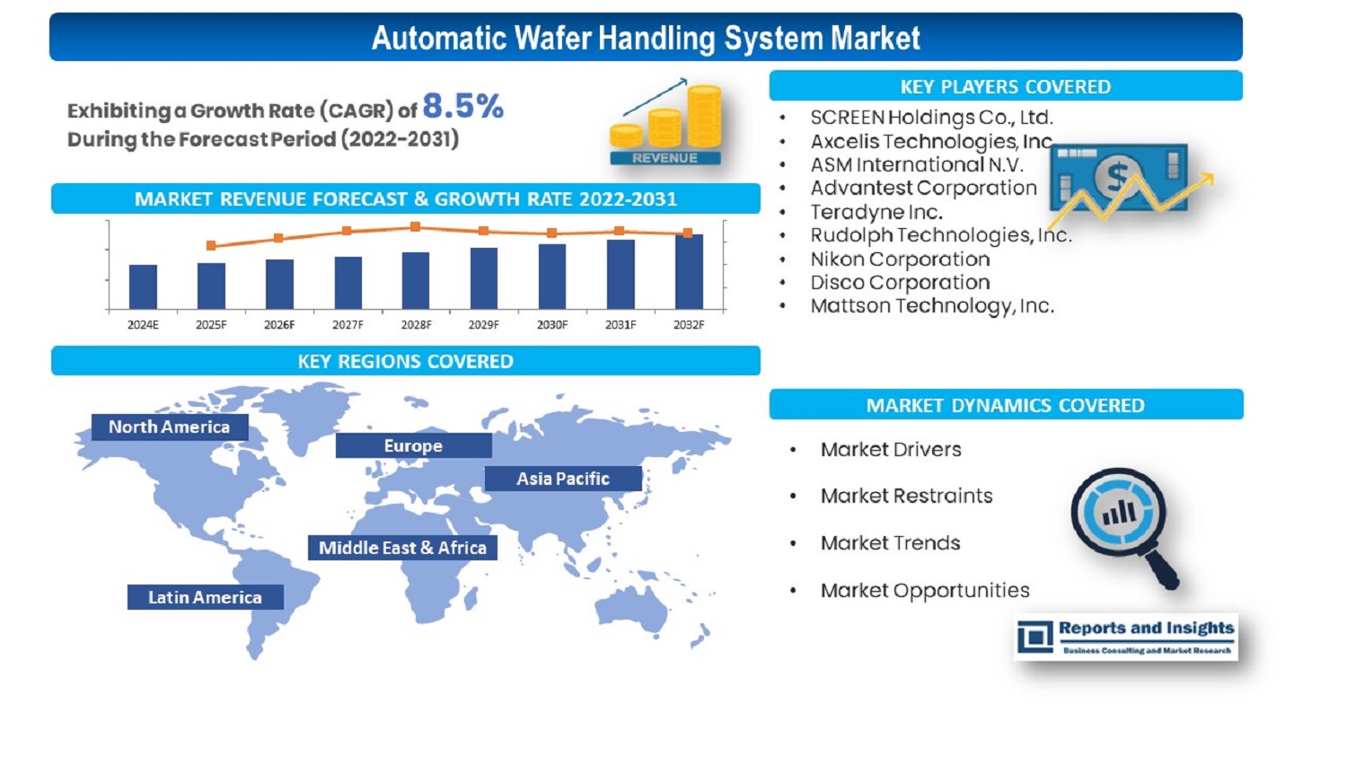
The semiconductor industry has witnessed a surge in demand for automation solutions, and the Automatic Wafer Handling System Market is no exception. This market revolves around the automation of processes related to the handling, transportation, and storage of wafers used in semiconductor fabrication. The increasing complexity and miniaturization of semiconductor devices have intensified the need for precise, high-speed, and reliable wafer handling systems.
The market is witnessing substantial growth due to factors such as the rise in demand for advanced electronic devices, the continuous evolution of semiconductor technologies, and the increasing focus on reducing manufacturing costs. Moreover, the shift towards 300mm wafer technology and the emergence of Industry 4.0 concepts are propelling the adoption of automatic wafer handling systems across the semiconductor manufacturing sector.
Request Sample Copy (To Understand the Complete Structure of this Report [Summary + TOC]): https://www.reportsandinsights.com/sample-request/1924
Segmentation:
The Automatic Wafer Handling System Market can be segmented based on various criteria, including system type, application, and region.
- System Type:
- Robotic Handling Systems: These systems utilize robotic arms equipped with advanced end-effectors to pick, place, and transport wafers.
- Fixed Handling Systems: These systems consist of stationary platforms and conveyor belts for wafer transportation within the manufacturing facility.
- Application:
- Front-End Semiconductor Manufacturing: Involves wafer handling during the fabrication of semiconductor devices.
- Back-End Semiconductor Manufacturing: Encompasses processes like packaging, testing, and assembly.
- Region:
- North America: Dominated by established semiconductor manufacturers and technological innovators.
- Asia-Pacific: A key region due to the presence of major semiconductor manufacturing hubs, especially in countries like China, Taiwan, and South Korea.
- Europe: Witnessing steady growth in the adoption of automatic wafer handling systems.
Segment Analysis:
Robotic Handling Systems Lead the Way: Robotic handling systems are emerging as the dominant segment in the Automatic Wafer Handling System Market. The ability of robotic arms to perform complex tasks with speed and precision aligns well with the requirements of modern semiconductor manufacturing. These systems not only enhance efficiency but also contribute to the reduction of human errors, leading to improved yield rates in semiconductor production.
Front-End vs. Back-End Application: The front-end semiconductor manufacturing segment holds a significant share in the market, driven by the increasing demand for advanced semiconductor devices. The need for automated handling solutions is particularly pronounced in processes like lithography, etching, and deposition. However, the back-end application segment is catching up as semiconductor packaging and testing processes become more sophisticated, demanding precise wafer handling.
Top Key Players:
The Automatic Wafer Handling System Market is characterized by intense competition, with several key players shaping the industry landscape. Among the frontrunners are:
- Brooks Automation, Inc.: A global leader offering a comprehensive range of automation solutions for semiconductor manufacturing, with a strong focus on innovative wafer handling systems.
- Applied Materials, Inc.: Renowned for its cutting-edge technology solutions, Applied Materials plays a pivotal role in the development of wafer handling systems for both front-end and back-end semiconductor processes.
- KUKA AG: Leveraging its expertise in industrial robotics, KUKA has established itself as a key player in the market, providing advanced robotic handling solutions tailored for semiconductor applications.
- Asyst Technologies (A Subsidiary of MIRAE Corporation): A major player specializing in automation and robotics, Asyst Technologies brings a diverse portfolio of wafer handling solutions to the market.
Request Sample Copy (To Understand the Complete Structure of this Report [Summary + TOC]): https://www.reportsandinsights.com/sample-request/1924
About Reports and Insights:
Reports and Insights is one of the leading market research companies which offers syndicate and consulting research around the globe. At Reports and Insights, we adhere to the client needs and regularly ponder to bring out more valuable and real outcomes for our customers. We are equipped with strategically enhanced group of researchers and analysts that redefines and stabilizes the business polarity in different categorical dimensions of the market.
Contact Us
Reports and Insights
Tel: +1 347 748 1518